Showing posts with label PCB assembly process. Show all posts

Sunday, April 25, 2010

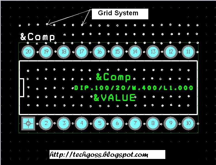
Parameters of Layout Check while Designing a PCB : 2 [ Grid System]


Grid system is basically required to get an accuracy while drawing the hole location of a component. The use of grid gives more convenience in placement of components and conductors on the PCB. It is a general practice to use grid system in layout designing.

By using the grid system in the artwork preparation stage the pads can be placed at exactly the center of the grid intersection. In the modern times the grid system is present in your PCB designing software itself. Using a grid of 100mil is adequate. But if you wanna shrink your PCB then grid of 50mil is also acceptable.

As the design becomes more and more complex finer and finer grids are required. Universal  grid system is based on the 0.05mm unit. For all shape and sizes and for every aspect of the PCB layout grid size should be incremented as the multiple of  5; else routing will be quite difficult.

Want to know more about grid system PCB design org >>
read more...

Sunday, April 11, 2010

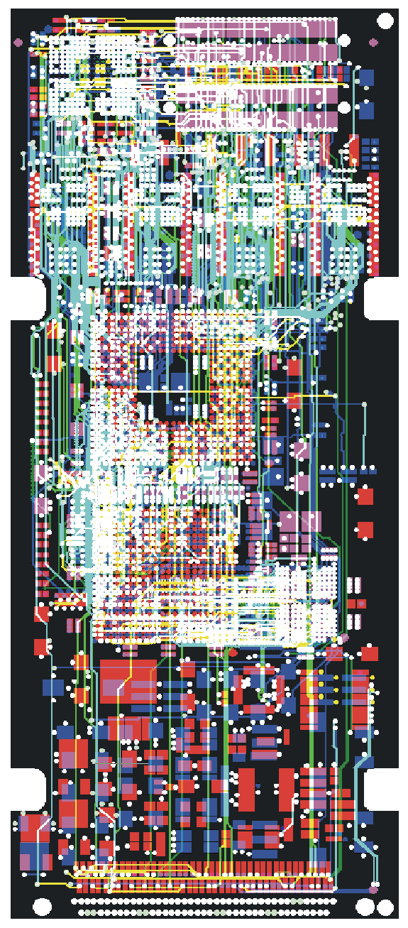
Optimum Package Density of PCB.

Components Package Density
An optimum package density of a printed circuit board results into better electronics performance at a reduced cost and gives the impression of an optimum design. The package density is linked with many constraints.

- Purpose & use of the equipment whether airborne, portable or permanent/ fixed installation.

- Heat produced and cooling provisions that is whether hermetically sealed, natural air flow, forced cooling.

- Types of components on the board; silicon devices have a shorter life, higher the temperature.

- Types of PCB used that is whether single sided, double sided or multilayer PCB.

- Component technology used whether discrete semiconductor, SSI, LSI.

The density of a board can be measured by the number of connections per square inch or the pad count per square inch. Connections between 65 to 120 is considered dense.

Package density is important to be considered in the earlier stages of design process. It is because if the density is very low, more PCB's will be used to realize the same circuit. This will result into more volume of the equipment, more PCB connectors & back panel wiring with more parasitic influences on working Circuit.

read more...