


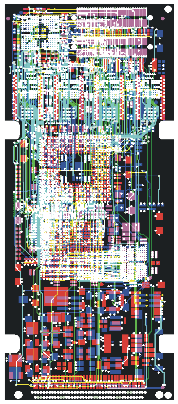
An optimum package density of a printed circuit board results into better electronics performance at a reduced cost and gives the impression of an optimum design. The package density is linked with many constraints.
 - Purpose & use of the equipment whether airborne, portable or permanent/ fixed installation.
- Heat produced and cooling provisions that is whether hermetically sealed, natural air flow, forced cooling.
- Types of components on the board; silicon devices have a shorter life, higher the temperature.
- Types of PCB used that is whether single sided, double sided or multilayer PCB.
- Component technology used whether discrete semiconductor, SSI, LSI.
The density of a board can be measured by the number of connections per square inch or the pad count per square inch. Connections between 65 to 120 is considered dense.
Package density is important to be considered in the earlier stages of design process. It is because if the density is very low, more PCB's will be used to realize the same circuit. This will result into more volume of the equipment, more PCB connectors & back panel wiring with more parasitic influences on working Circuit.


")


0 comments: on "Optimum Package Density of PCB."
Post a Comment