

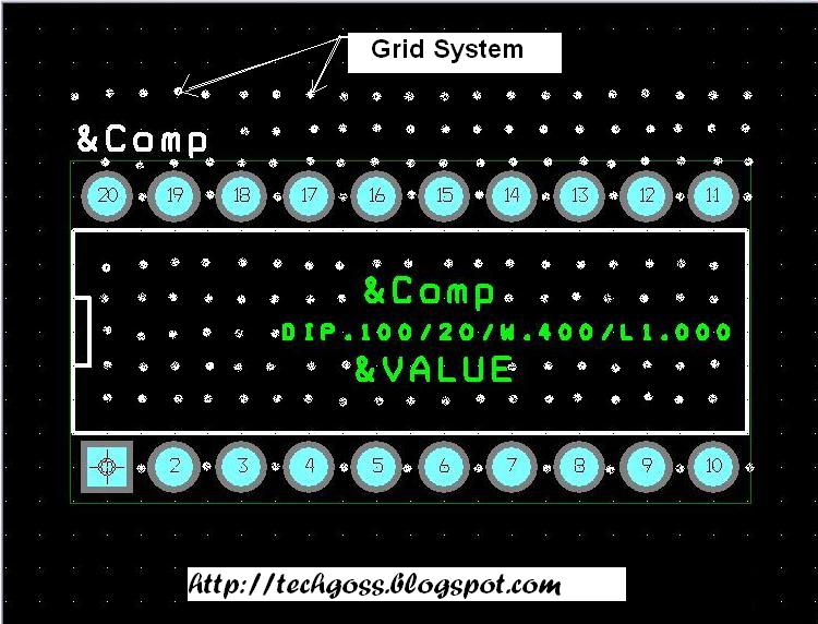
Grid system is basically required to get an accuracy while drawing the hole location of a component. The use of grid gives more convenience in placement of components and conductors on the PCB. It is a general practice to use grid system in layout designing.

By using the grid system in the artwork preparation stage the pads can be placed at exactly the center of the grid intersection. In the modern times the grid system is present in your PCB designing software itself. Using a grid of 100mil is adequate. But if you wanna shrink your PCB then grid of 50mil is also acceptable.
As the design becomes more and more complex finer and finer grids are required. Universal grid system is based on the 0.05mm unit. For all shape and sizes and for every aspect of the PCB layout grid size should be incremented as the multiple of 5; else routing will be quite difficult.
Want to know more about grid system PCB design org >>
Want to know more about grid system PCB design org >>


")


0 comments: on "Parameters of Layout Check while Designing a PCB : 2 [ Grid System]"
Post a Comment