Tuesday, June 1, 2010

Peering Into Reverse Engineering


Have you ever thought of buying an Ipad or Iphone and tear it down into pieces to peer inside its integrated circuits and processor. No! I know you are not that Einstein. But researchers form chipwork make it their business to find it out. They buy mobile phones, laptops and reverse engineer the hardware, ICs and derive the complete schematic diagram.

Actually the reverse engg. process has long been recognized in semiconductor industry. For example to get a piece of silicon from plastic package, is dipped into a beaker of acid. For ceramic and metal can packages different complicated process are followed. 

So what new reverse engineers found after tearing down Ipad was 16Gbyte memory powered by two Samsung K9LCG08U1M 8Gbyte flash Nand memories; and instead of  Texas Instrument's touch controller do all the touch screen controls as in Iphone 3G they used three- chips as their earlier version of Iphone 2G.


Image: Inside Apple Ipad a)Metal Layers b)Transistor details c)Circuit Layout.

But the most difficult portion is to peer into smaller and delicate designs. With the use of powerful electron microscopes like SEMs (scanning electron microscope) and TEMs (transmission electron microscope) magnification till atomic level is feasible. With the analysis of cross-section and planar section of the layers, images are merged in a software like ICwork and a schematic is obtained.


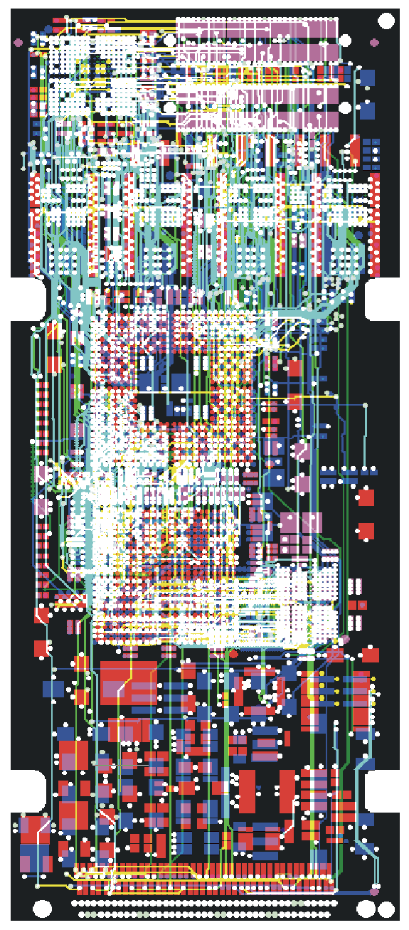
Image: Schematic obtained of Bootstrap Oscillator circuit from SmartMOS DC/DC converter

But a question still arises whether reverse engg. is legal. In US according to Semiconductor Chip protection act the technique is allowed for the purpose of teaching, analyzing and evaluating the concept. Similar law exists in European Union, Japan and other jurisdiction. But with the growing competitive intelligence people involved in patenting are evolving with new techniques and designs which are hard to debug and reverse engineer.

read more...

Saturday, May 1, 2010

Generate Electricity With Every Move You Make Every Step You Take.


Have you ever wondered generating electricity merely by walking over a distance. If not then you will be amazed to know that scientist from Georgia tech University has developed a device which can generate power from body movement.

They have used Piezoelectric materials and drawn them into nanowires that can be woven into cotton shirt or housed into shoe hill. Piezoelectric crystals have a special characteristic that when they are subjected to force or pressure they produce electric signals. Though this electric signals are very weak but by cramming 20,000 nanowires into three square cm area can produce power in millivolt range.

With every move and every step you take pressure is applied on the piezoelectric crystal and electric signal starts flowing through the electrodes. It may not be possible to turn on an electrical appliance but at least atleast cellphones and ipods can be easily charged.


Single nanowires are invisible to naked eyes. Prof Z.L.Wang and his team at Georgia tech are using Zinc Oxide nanowires to built this nano generators. This nanowires are 50 to 200 nanometers in diameter and 5 micron in length. 2 thin electrodes are used and place between this 20,000 nanowires to drive current from it.

This arrangement helps to maximize the electricity produced by piezoelectric crystals. But if the zinc oxide is replaced by Gallium Nitride the power output could increase by 10 times.

If the device is not in constant motion then the nanowires will shut off and no electricity will flow. To rectify this Prof. Wang will develop supercapacitors to store the charge generated by the nanowires. 

Till now only a prototype is made and lots of work is needed to be done. It is likely to take 3-4 years before you can actually get a cloth of nanowires and put the concept into action. Till the time hold on and wait...
read more...

Sunday, April 25, 2010

Parameters of Layout Check while Designing a PCB : 2 [ Grid System]


Grid system is basically required to get an accuracy while drawing the hole location of a component. The use of grid gives more convenience in placement of components and conductors on the PCB. It is a general practice to use grid system in layout designing.

By using the grid system in the artwork preparation stage the pads can be placed at exactly the center of the grid intersection. In the modern times the grid system is present in your PCB designing software itself. Using a grid of 100mil is adequate. But if you wanna shrink your PCB then grid of 50mil is also acceptable.

As the design becomes more and more complex finer and finer grids are required. Universal  grid system is based on the 0.05mm unit. For all shape and sizes and for every aspect of the PCB layout grid size should be incremented as the multiple of  5; else routing will be quite difficult.

Want to know more about grid system PCB design org >>
read more...

Guide To Conquer Electronics [Resistors]


Resistors are the simplest components of electronics. There's nothing great that you may find difficult to understand. Moreover there are tons of sites on the net that are loaded with the of concept of resistors. But one thing which  I have found similar in all these sites are; they discuss about what the resistors actually are and how we can determine the color codes. But none of them discuss about the different types of resistors and which type of resistor should be used where. 

So I decided to come up with a Guide to Conquer Electronics with an idea to explore the applications of different components of electronics and their types.

While designing a circuit it is very important to maintain proper current and voltage level across different components for proper operation of the circuit. If excess of current is flowing then it can be brought down using resistors. Resistors are available in different ohm ratings and different wattage.


The guide covers all this subjects with a pictorial representation. Pictures will help you for the better identification of the component, its package type, and space required on the PCB.  I hope the Guide to Conquer Electronics will be advantageous  for you in better circuit designing.
If you are unable to understand the concepts of electronics like JFETs, voltage regulators, Ac modeling then we have electronic movies a fully animated program in store for you. Visit EMovies >>

read more...

Wednesday, April 21, 2010

Evoulation of Radio Astronomy: The Complete Story.


The age of radio astronomy began from the day when engineers learned to generate radio waves using an electron tube. Approximately after a decade from the discovery two young and dynamic engineers Gregory Breit and Merle Tuve, bounced radio waves off the ionosphere and determined the height of the layers. This proved that radio waves can travel beyond earth and back and they can be used as a probe for communication. 


Two years later a well known American inventor, writer, and magazine publisher Hugo Gernsback popularly known as father of science friction proposed an article "Can We Radio The Planets". The radio waves that can be bounced from the moon and the planets. He also stated that 2.5sec will be required for a radio wave to travel to the moon and back.


In the years of 1930 Karl Guthe Jansky at Bell Telephone Laboratories investigated the noise sources in radio transmission. Jansky used a large directional antenna of 14.6m wavelength which identified three different types of static noise. Noise signal from local thunderstorms, a steadier (ie; firm in position) and weaker static from distant thunderstorm and a weak hiss from unknown source. 

The weak signal from the unknown origin peaked about every 24 hours. Firstly Jansky suspected that this unknown source was sun crossing the view of his directional antenna, but when Jansky compared his observations with the optical astronomical maps, he concluded that the radiation was coming from the Milky Way and it was maximum in the direction of center of galaxy.

But instead of encouraging the research of Jansky; Bell's laboratory rejected Jansky's request to build a 100 foot radio telescope. No other institution followed Jansky's work.

Only after World War II a radio engineer Grote Reber took Jansky's work and continued it as a hobby in his spare time. He built a 31-foot parabolic antenna and in 1937 made the first radio map of the sky. With the intense development of radar technology during the world War II gave a new aid to astronomers. 

 
A team headed by J.H. De Witt of U.S. Army Signal Corps were succeeded in seeing the echoes of the moon on the cathode ray tube .
From then there was no turning back and in the years of 1940-50 radio astronomy emerged as a new branch of astronomy. A 76m steerable radio telescope was built in England at Jodrell bank in 1957. 


While a 305 meter fixed reflector was completed in Arecibo Puerto Rico in 1963. It is the world's largest radio telescope made till date.

read more...

Saturday, April 17, 2010

Parameters of Layout Check while Designing a PCB : 1 [ Layout Scale ]


The layout of a PCB has to incorporate all the information on the board before one can go on to the artwork preparation. Layout check is a concept which clearly defines all the details of the circuit & partly also of final equipment. It is a prerequisite before the actual layout can start.
For a design engineer the parameters to be considered for planning the layout of a circuit includes layout scale, grid system, board types, circuit diagram, component list, layout sketch, artwork preparation, component mounting, layout check, resistance, inductance, and capacitance. Let us see how we can implement this parameters effectively while designing a PCB layout. A series of post will cover every single topic mentioned above.

< Layout scale >
Depending on the accuracy required, artwork should be produced at a 1:1 or 2:1 or even 4:1 scale. The layout is best when prepared on the same scale as artwork. 

If you didn't understand what this means, then consider an example. Suppose your desktop wallpaper's resolution is  1024 x 768. And let us say this resolution signifies a normal ie; 1:1 scale for your desktop. But at the same time you can also zoom the wallpaper to say 1600 x 1200 representing a 2:1 scale. Thus this scale represents nothing but a zoomed version of your artwork.

layout scale

A 2:1 artwork has 4x actual PCB area and a 4:1 artwork has 16x the PCB area. Normally a 1:1 scale is considered while transferring the artwork on the PCB.


read more...

Sunday, April 11, 2010

Optimum Package Density of PCB.

Components Package Density
An optimum package density of a printed circuit board results into better electronics performance at a reduced cost and gives the impression of an optimum design. The package density is linked with many constraints.

- Purpose & use of the equipment whether airborne, portable or permanent/ fixed installation.

- Heat produced and cooling provisions that is whether hermetically sealed, natural air flow, forced cooling.

- Types of components on the board; silicon devices have a shorter life, higher the temperature.

- Types of PCB used that is whether single sided, double sided or multilayer PCB.

- Component technology used whether discrete semiconductor, SSI, LSI.

The density of a board can be measured by the number of connections per square inch or the pad count per square inch. Connections between 65 to 120 is considered dense.

Package density is important to be considered in the earlier stages of design process. It is because if the density is very low, more PCB's will be used to realize the same circuit. This will result into more volume of the equipment, more PCB connectors & back panel wiring with more parasitic influences on working Circuit.

read more...